
Sequential Optimal Packing for PCB Placement
A simple deterministic packing strategy that benefits from feedback loops

Placing chips on a PCB is a difficult and consequential task. The way you place chips dramatically impacts how difficult it will be to route the PCB. There are signal integrity and power management issues with creating long paths between different components. The size of the PCB or where ports appear often is a design requirement that has to be considered and in some cases- pushed back on.
How does automatic placement fare? If you use a regular packing algorithm that minimizes the space usage, you will create a board that is nearly impossible to route. If you use a force-directed packing, where the netlist forms springs that pull chips close together based on their connections, you’ll get an unusual shape and suffer local minimums (it’s also wildly unpredictable)
When we’re thinking about packing algorithms, the first concern should be capturing human design requirements. The algorithm should, as closely as possible, understand statements like:
The USB port must be 2mm from the left edge on the top side
The decoupling capacitors must be near the power pins on the microcontroller
The left and right headers must be spaced 20mm apart, and aligned
Copy the placement from the datasheet EXACTLY for this subcircuit
How do we capture these requirements? In tscircuit, they are captured through <group>/<subcircuit> tags with different layoutMode properties, also coordinate specifications like pcbLeftEdgeX=calc(board.minx + 2mm). In some cases, the entire layout can be resolved by ordering the computations properly, but more often than not, this way of specification is arduous for the user and inflexible as a design grows.
For underspecified placements, Sequential Optimal Packing is a fast, deterministic and legible solution for packing. It allows us to capture “flexible” design constraints in a predictable way.
Sequential Optimal Packing
Sequential Optimal packing sequentially packs chips in the Pack Order. Each time it packs a new chip, it selects the Optimal position based on the Cost Function. The Cost Function is established from the design intent for that specific chip.
Here’s the algorithm in a nutshell:
Order your chips in the Pack Order
If there are no preplaced chips, pack the first chip in the center
Main Loop:
Pick the next chip
Find the optimal placement and rotation for that chip and place
Repeat until all chips are packed
Simple!
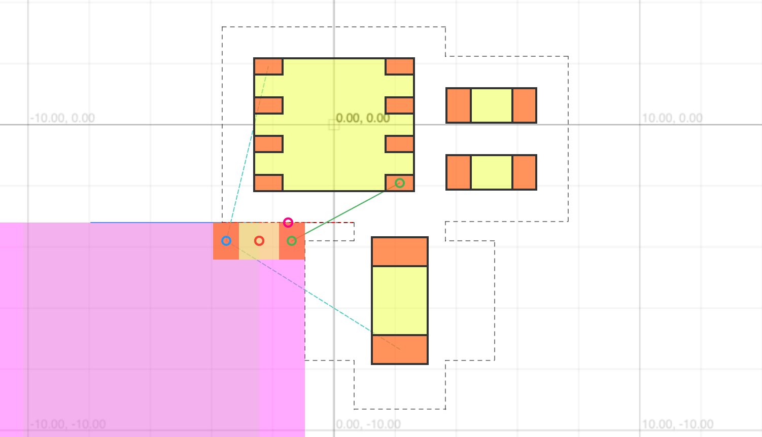
This algorithm can be made fast because you can quickly compute a boundary along our existing packed chips and pads, then find the Cost Function minimum along each segment of the boundary.
In the animation below, you can see the algorithm in action. The lines from pin to pad help show what the components of the Cost Function are. You can think of the Cost Function as “summing” the lengths of all the lines or taking the minimum of all the line lengths as the cost.
Sequential Optimal Packing is great
Sequential optimal packing is easy to understand and visualize. You can easily watch each component pack one by one and vary the pack order or optimal packing function to achieve a desired outcome. Every individual packing decision is easy to understand.
If you are using tscircuit, you can debug the packing algorithm using the “Solvers” tab.
Sequential optimal packing is also extremely compatible with other layout mechanisms, like when you want to have a group of components that are in a reference configuration (from a datasheet) but should be packed together. You can also layout pre-computed positions before you begin packing- it’s compatible with partially packed existing layouts.
Downsides
Sequential optimal packing is flawed in two major ways:
The best pack order is not initially obvious, early chips can be placed such that later chips don’t pack well
Sometimes the global optimal placement is impossible, because it requires two chips to be packed in locally sub-optimal positions
Both of these issues can be mitigated by treating sequential optimal placements as an initial approximation, then refining by “hardening” constraints. e.g. if you know you want a decoupling capacitor in an exact position relative to a chip, encode that such that the chip and decoupling capacitor are packed together. LLM loops can easily adapt the design intent representation to do this!
Conclusion
Sequential Optimal Packing is one of the key algorithms that should be included in the standard constraint algorithms for PCB design. It is highly debuggable, easy to understand, and can be tweaked in a feedback loop until you reach a global optimal placement. It should be a fundamental algorithm, similar to flexbox or CSS Grid, baked into every PCB engine.
If you’re interested in algorithm development, join our discord or follow me on twitter.